Frequently Asked Questions
The Market
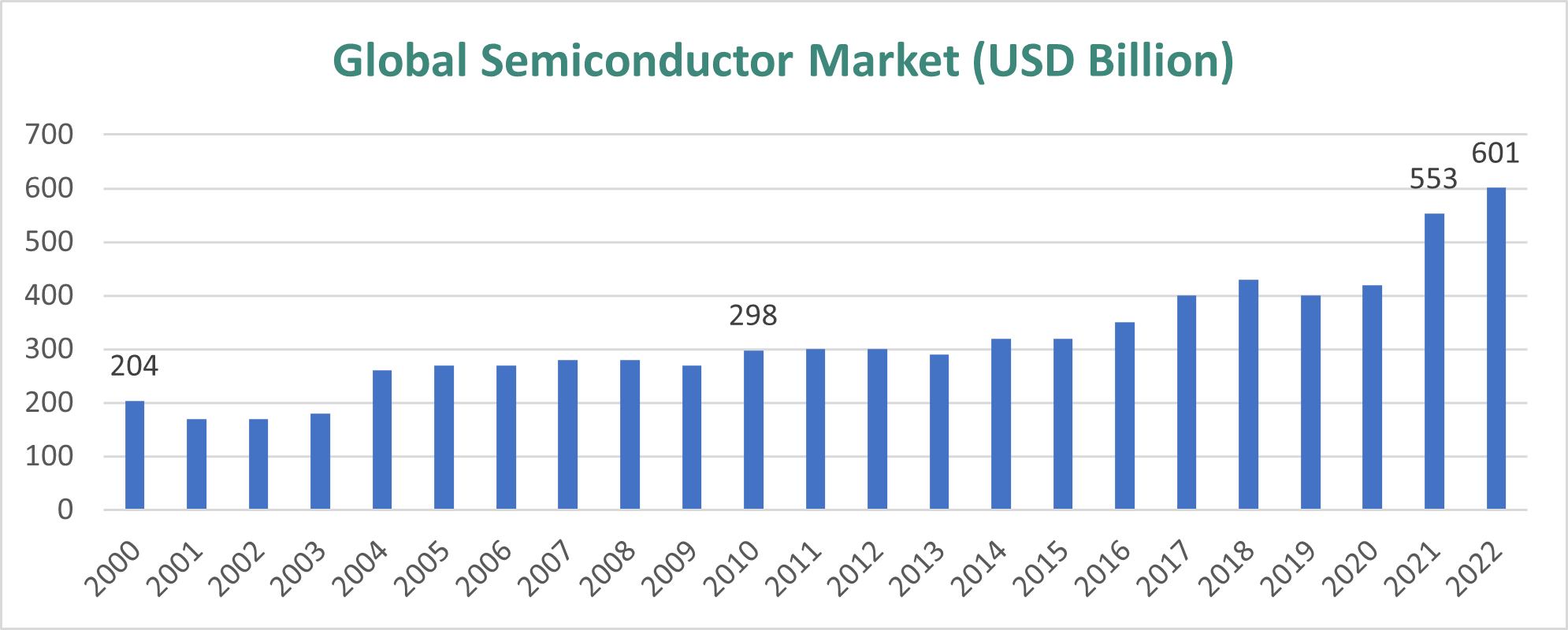
The global semiconductor market has grown substantially from $298 billion in 2010 to $553 billion in 2021. It is expected that the market will surpass $600 billion in 2022. The semiconductor industry’s
Compounded Annual Growth Rate (CAGR) for 2021 to 2026 is estimated to be 7.1%.
Chart: Global Semiconductor Market (2000-2022)
Produced semiconductors are being used in the following sectors:
– Computing
33%
– Communications
31%
– Consumer electronics
12%
– Industrial, military & aerospace
12%
– Automotives
11%
– Others
1%
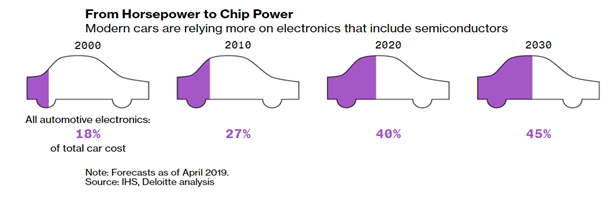
It should be noted that the usage of chips in some industries, such as the automotive sector, has increased significantly and is expected to continue, especially with the emergence of autonomous driving vehicles. It seems that the industry is changing its slogan from horsepower to chip power. Modern cars are relying more on electronics that include semiconductors. The following graph depicts the growing share of the value of electronic parts in a car.
Most fabrications are done by foundries, which specialize in the manufacturing of chips based on design and specifications of fabless companies and are mostly located in Asia. The top foundries in 2021 were in:
– Taiwan
63%
– South Korea
17%
– China
7%
– US
7%
– Others
6%
Taiwan Semiconductor Manufacturing Company (TSMC) is the biggest foundry in the world and manufactures 54% of all chips. Other most important foundries include UMC (Taiwan) and GlobalFoundries (USA).
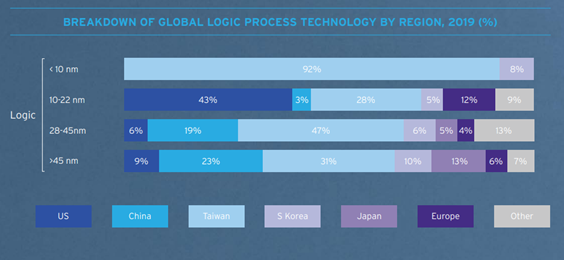
Breakdown of global chips production by size and region
Fabless companies design their products and give the specifications and orders to foundries to fabricate. The chips produced in 2021 belonged to companies in the following countries:
– USA
47%
– South Korea
20%
– Japan
10%
– EU
10%
– Taiwan
7%
– China
5%
– Others
1%
Most important fabless companies include AMD, Nvidia, and Qualcomm.
Yes, Integrated Device Manufacturer (IDM) is a semiconductor company which designs, manufactures, and sells its own chips. The most prominent IDMs are Intel, Samsung, and Texas Instruments.
In 2021, semiconductor companies worldwide spent $146 billion building new production capacity and on research, according to research firm Gartner. TSMC, Samsung and Intel — three of the world’s biggest chipmakers — accounted for 60% of the $146 billion.
Future investment of the power trio continues:
– Samsung is investing $150 billion in its logic chip and foundry sector, to be the top logic chip maker, by 2030.
– Intel is currently making investment of more than $20 billion in the construction of two new leading-edge chip factories in the US. It also plans to invest as much as 80 billion euros in Europe over the next decade to boost the region’s chip capacity and will open its semiconductor plant in Ireland for automakers.
– The world’s largest contract chipmaker, TSMC, has committed to investing $100 billion over three years to ramp up production. It is also building a $12 billion 5-nanometer chip fabrication plant in Phoenix, Arizona.
Since the beginning of the chips shortage, governments have been active in facilitating the growth of the semiconductor industry and do what they can to decrease the supply and demand gap. Governments have realized that recent incidents (worldwide corona outbreak, Russia-Ukraine conflict, and Taiwan’s not so secured sovereignty) can easily affect the chips market and as a result the global economy.
This was felt so much that the US and EU announced their own Chips Acts.
US Chips Act: The US passed in 2021, a law that would provide chipmakers with $52 billion in subsidies to advance semiconductor manufacturing. The aim is to boost and enable the establishment of more production capacity within the country to become less dependent on foreign suppliers.
EU’s New Chips Act: Ratified in 2022, EU woes to invest €43 billion in 10 years in an attempt to secure its supply chains, avert shortages of semiconductors in the future, and promote investment into the industry. The plan is to increase EU’s share from currently 10% of global semiconductor industry to 20% in 10 years. Given the fact that the whole market will double in 10 years, it would mean that EU has to quadruple its production in order to reach its goal.
Similar subsidies and support programs have been introduced in other countries such as China, and South Korea.
South Korea also wants to become the world’s biggest chip producer, with companies and the government pouring a total $450 billion into the industry by 2030.
China has already been spending what could amount to $150 billion by 2030 to jumpstart production. The country is still far behind, especially when it comes to advanced chip making, but it’s catching up quickly.
There are currently various programs that offer grants and subsidies to semiconductor manufacturers, research institutes and start-ups. The most prominent ones are:
Digital Europe – This Fund is focused on bringing digital technology, especially high-performance computing, to businesses, citizens and public administrations. The allocated resources for Digital Europe Program are €7.5 billion. Digital Europe has many programs that are specific and related to the optimization of the semiconductor industry.
EU Green Deal – The objective is for the EU to become the first climate neutral continent by 2050, resulting in a cleaner environment, more affordable energy, smarter transport, new jobs and an overall better quality of life. Sustainable Europe Investment Plan (SEIP) aims to mobilize at least €1 trillion in sustainable investments by 2030. Since energy-efficiency of semiconductors would be a major factor, the stakeholders in this industry are entitled to grants and funds.
Multi-Purpose Sensor
Existing Problems: Current detection mechanisms use chemical processes to determine the existence of a pathogen or a virus. As a result, a lot of material is used, and the testing kit can only be used once leading to a high cost and waste. Also, for each virus new chemicals and testing kits and instructions need to be provided. The consequences are:
– Bad for the environment: The chemicals and kits are wasted and not easily recyclable
– Too costly:
o Equipment: For each test a new kit and equipment is needed
o Tests: New tests need to be developed for each pathogen
– High response time: Obtaining the test result is time consuming
Our solution: Our semiconductor biosensor doesn’t use chemicals, provides the results within seconds and can be programmed to detect any pathogen or virus without any limitations on the number of times they can be used.
Additional applications: The device can be used for identification of any liquid and is not limited to pathogens. Among its other applications the following can be mentioned:
– Medical applications:
o Blood analysis: It can be programmed to determine the level of sugar or cholesterol in blood samples.
o Cancer: It can identify the change in cancer cells after chemotherapy
– Food industry: An easy and fast way of checking any type of liquid food for its freshness and health
– Agricultural sector: Determining ripeness, level of chemicals, soil examination
– Boarder and customs: Examination for illegal substance contamination
Conventional practical detectors are normally chemical based. Ours work based on the physical characteristics of any material. Specifically, it measures the placement of atoms in the molecule of viruses. The placement of atoms in a virus acts as an identifying fingerprint and this makes detection very accurate, and the result is available in seconds.
Reusable: Our device can be used thousands of times. A ten thousand test cycles would be minimum.
Programmable: Through its accompanying software application, the device can be programmed to detect any virus or pathogen.
Fast and convenient: Detection occurs only in a few seconds and the result is stored in a computer. The device would be ready for another test withing a couple of minutes after wash and rinse.
Low temperature functionality: Our device is also suitable for gas detection at low temperatures. Gas detectors normally operate at elevated temperatures, which makes them especially impractical for space or combustible environments. Our detector can operate at any temperature down to zero kelvin.
The device is basically a specialized Schottky junction, whose manufacturing is much less complicated and less costly compared to those of any other semiconductor biosensor.
– Current producers of detectors can buy license to our technology and start utilizing our solution into their products and brands (Metrohm AG, Innovate Sensor Technology AG, Enoveo…)
– Major companies within:
o Pharmaceutical (Roche, Merck, Pfizer, Sanofi…)
o Medica and Pharmaceutical (Abbot, Medtroncis, GE…)
o FMCG companies (Johnson & Johnson, P&G, Unilever…)
o Petrochemical companies (Shell, BP Petrochemicals…)
Innovative JFET
Existing Problems: The state-of-the-art technology for manufacturing CMOS has faced a challenge with regards to downscaling this type of transistor below 2-5 nanometre range. Also, the power consumption of these transistors needs to be decreased if further downscaling is to occur. It is also desirable to achieve higher frequencies in microprocessors – something that has remained dormant for several years now.
Our Solution: Our modified JFET addresses all these problems! It can be downscaled below 2nm without suffering the problems that CMOS has at these dimensions. Its power consumption is one tenth of CMOS transistors. Its speed is estimated to be at least 3 times faster than CMOS transistors.
Additional application usage: Our modified JFET transistors are optimal for supercomputer and space-based electronics as they:
· perform better at lower temperatures (supercomputers are normally cooled);
· are more resilient against solar radiation;
· are less noisy requiring less power transmit/receive information; and
· consume much less energy that makes them optimum for these two applications.
In our novel design, the Source and the Drain terminals do not need to reach (touch) the Gate connection. This approach eliminates several processing steps and allows for much smaller transistors to be fitted in advanced processors. This allows it to be operational at 1nm gate length. Manufacturing of our JFET is less time consuming and less expensive since some steps are not needed in our design.
Both voltage polarities: Our modified JFET can tolerate both voltage polarities at its input, unlike a regular JFET that can only accept one voltage polarity. If a different voltage polarity is applied to its input the device allows a very large current to flow from the input into the output either burning the transistor and its associated circuits or interfering with its operation in the best-case scenario.
Lack of current leakage: Our modified JFET eliminated the so-called input or gate current leakage that plagues all JFET transistors including HEMTs. As such it helps with the power consumption of the device; furthermore, in digital applications the power consumption of this transistor is relatively less compared to other types of transistors.
Digital performance: Unlike regular JFTEs, our modified version operates as a digital switch with all the performance characteristic that are needed for a viable microprocessor chip.
Analogue and digital: The fact that our transistor can operate with both voltage polarities, makes it possible to be used in analogue as well as digital applications.
Due to the limitations of JFET models, CMOS transistors are the most used types in chips. However, our modified JFET performs all the functions of CMOS and in addition has the following advantages:
Power efficiency: Compared to the state-of-the-art CMOS transistors and circuits, our JFET solutions can operate at lower voltage and current levels, meaning that they consume much less power.
Higher frequency of operation: Our modified JFET is intrinsically faster than CMOS transistors for two basic reasons. First the speed of electrons is higher secondly because parasitic capacitances are negligible compared to CMOS models.
Signal to noise ratio– The signal to noise ratio of our JFET is much better than CMOS. This means less power is necessary to transmit and read information from each transistor and much weaker signals can be amplified by these transistors.
Less fabrication steps: Our modified JFET is easier to fabricate than a CMOS (MOSFET). Our nanometre size modified JFET eliminates 4 unnecessary and expensive fabrication steps of CMOS manufacturing. These steps are currently proprietary and belong exclusively to certain manufacturers.
Easier to downscale: Our modified JFET does not suffer from the nanometre size consequences that hamper the performance of CMOS. As a result, it can be downscaled by less expensive equipment. As is shown in Figure 1, the very fact that the source and drain do not need to touch the gate makes it possible to downsize the gate as much as technology allows without worrying that this brings the source and the drain closer to each other. The closeness of the source and drain causes all the problems for CMOS devices. Here we can keep the source and drain at a safe distance and decrease the size of the gate which determines the speed of the device. The size of a transistor is the critical dimension that determines its speed.
Most transistors used in advanced processors are within the 5-10 nanometres gate sizes. Our transistor has the potential to be downscaled to below 2 nanometres.
Theoretically, it consumes only one tenth (1/10) of energy compared to conventional transistors.
Our transistor has the potential to be 3 times faster compared to its CMOS counterparts.
Its fabrication eliminates several steps compared to conventional transistors and would allow existing manufacturers to revamp their production lines with minimum investments and produce much smaller and faster chips instead of setting up new production sites and fabrication lines.
Modified HEM
Existing Problems: Current HEMT transistors cannot be used in digital circuits. Furthermore, these transistors suffer from the current leakage that connects their input to their output.
Our solution: Our modified HEMT transistor solves both mentioned problems. In other words, it can be used in digital circuits, and it also eliminates the current leakage.
Additional application usage: The possibility of digital usage opens a whole new set of applications and markets. These include:
– Ultrafast microprocessors for computers and smartphones that could be 100 times faster than the conventional silicon ones. Such fast microprocessors can improve AI technology by the same factor.
– Medical applications in terms of non-invasive diagnostics becomes limitless.
– The space electronic market can be dominated by this technology in a decade, because of its resistance to radiation.
Our design only adds one additional fabrication step to HEMT manufacturing process. The step involves oxidising a metal layer, which is a standard process in semiconductor manufacturing. This additional step allows the HEMT transistor to act as a digital subcircuit.
Digital performance: Perhaps the most distinguishing comparison is that unlike regular HEMTs our modified version can operate as a digital switch with all the performance characteristics that are needed for a viable microprocessor chip. Our modified HEMT is appropriate for both analogue and digital applications.
Both voltage polarities: Our modified HEMT can tolerate both voltage polarities at its input. Regular HEMT that can only accept one voltage polarity at its input and if a different voltage polarity is applied to it, the transistor burns up or its operation is ruined.
Lack of current leakage: Our modified HEMT eliminates the so-called input or gate current leakage. As such it helps with the power consumption of the device; furthermore, the total power that it can deliver is larger for radar and power electronic applications.
Microprocessor application: Current HEMT transistors cannot be used to make a microprocessor, but with our modified HEMT we can manufacturer microprocessors which are much faster than existing CMOS transistors. For example, using InP [1] semiconductor compounds in our HEMTs results in digital circuits operating at 400 GHz frequency range. A frequency level that is unheard of and impossible to achieve by existing microprocessors based on CMOS transistors.
[1] Indium Phosphide
Our modified HEMT transistor has only one additional step to regular HEMT transistor manufacturing and the cost of the extra step is negligible because this step is already used in other parts of the process.
Superconductive Transistor
Quantum computing is the study of how to use phenomena in quantum physics to create new ways of computing. Quantum computing is made up of qubits. Unlike a normal computer bit, which can be 0 or 1, a qubit can be either of those, or a superposition of both 0 and 1.
Existing Problems: The building blocks of a quantum computer known as quantum bits need to be manipulated, their states need to be read or changed, and this is done via semiconductor transistor outside the quantum unit. The quantum unit is stored in a cryocooler with a temperature of -273° Celsius. The data needs to be transferred outside the cryocooler and then sent back via bulky connections, which leads to latency, higher costs, and bigger sizes of the unit. In general, today’s quantum computers consume too much energy, mostly due to the transfer of data between the cryocooler and semiconductors.
Our solution: Create digital and analogue circuits using innovative superconducting transistors alongside quantum bits. This will eliminate the need to send the signals outside the cryocooler and helps with speed and makes it possible to use millions of quantum bits instead of current tens of quantum bits.
Application usage: A huge market exists for quantum computers. Its economic justification based on our superconducting transistors, would create a vaster market for:
– Governments:
o Space and defence
o Social & economic planning
o Climate predictions
– Private sector:
o Automotive industry and autonomous driving
o Big data and data processing
o Financial markets projections
o Cyber security
So far only a handful of governments (the US, China, Russia…) and companies (Tesla, IBM, Google…) have their own quantum computers. As a more commercially viable product, there is no limit to its existing and emerging users.
[1] Transistor with zero electrical resistance
Amplification: Our superconductive transistor can amplify signals, which in electronic terms is known as gain. The current superconductive transistors are based on RSFQ [1] digital electronics, which does not produce any gain. Our device produces gain similar to a BJT transistor and hence it can be used in digital circuits.
Non-latching: Our transistor is non-latching like regular CMOS transistors, meaning that one can either turn it off or on with application of voltage to the input. The problem with current quantum computers is the latching to either on or off state.
Digital performance: For a transistor to perform well as a digital device it needs to possess specific characteristics. Our transistor has all these characteristics, which are the ability to amplify input signals, isolation of input and output, and the ability to connect to several transistors at its output. Therefore, the proper digital performance is predicted for our devices.
Analogue and digital: There is no superconductive transistor capable of both analogue and digital operations. Our solution can operate in both modes. This is very important when a practical electronic system is to be designed. There won’t be any need to use semiconductor transistor for any purpose in quantum computers.
[1] Rapid Signal Fluxon Quantum Logic
Our transistors are fabricated alongside the quantum bits with the same fabrication processes, so their fabrication cost would be the same. Furthermore, since our transistors eliminate the need to use HEMTs and CMOS processors, the total cost of a quantum computing unit would be a lot less if our transistors are used instead of the semiconductor transistors.